e-e-Paper Display Module
Hardware / Device Information
The assembled circuit board looks as below:
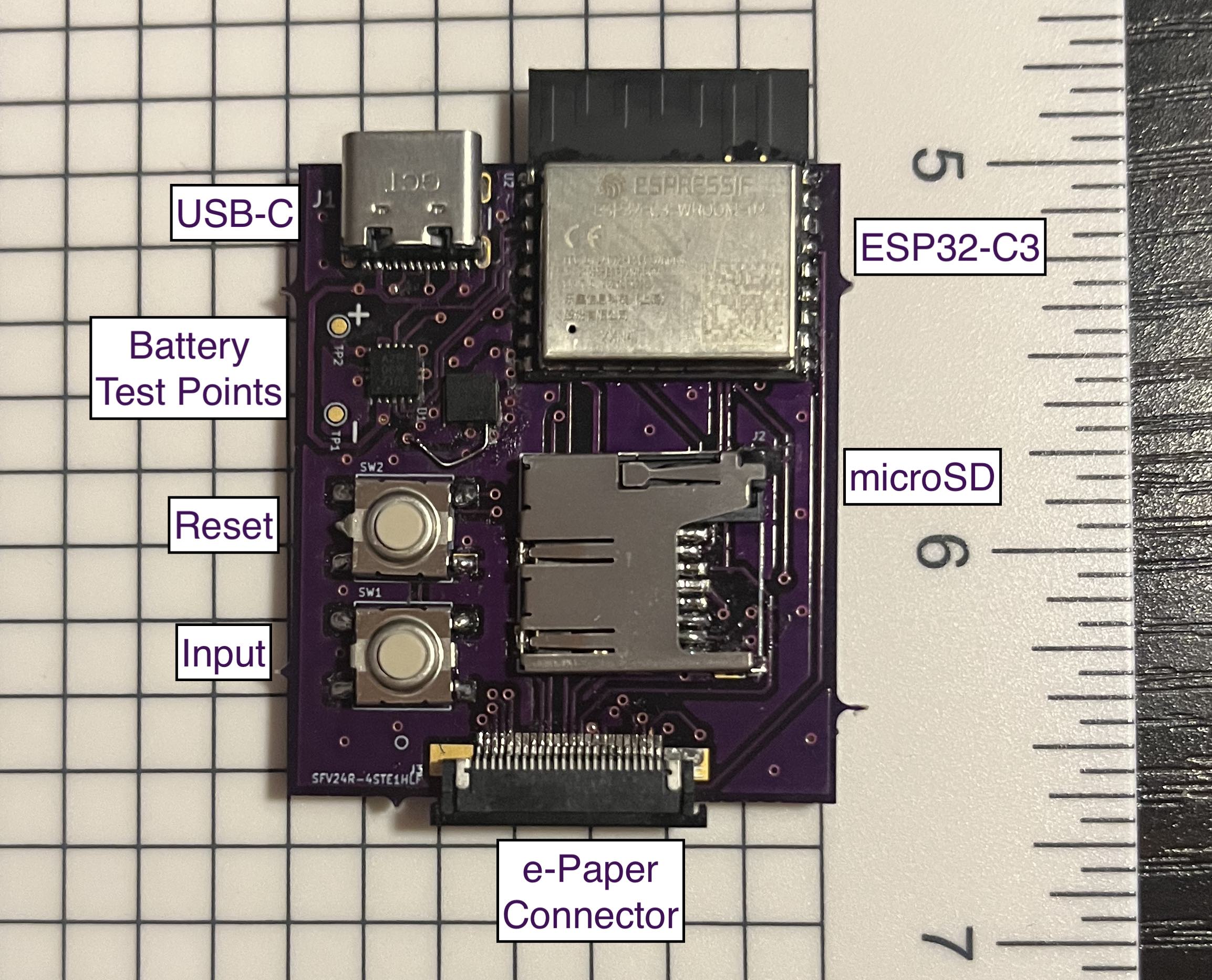
The other side of the board primarily has passives on it.
For reference, the output schematics, fabrication files (gerbers), and BOM from the initial schematics
are provided in the hardware/v1 folder of the repository.
Version 2 is now added, fixing many of the quirks listed below, but is in fab / not yet tested.
Quirks
There are a litany of small and large changes that will be fixed with a new design (most of these being from the prototype-like nature of v1):
- The pinout of the connector and display are in opposite order from intended, so the board folds in the wrong/unintended direction in an enclosure. Oops!
- The LDO symbol and layout could be adjusted for an enable version.
- The power/charging/LDO circuitry can probably be re-done to have lower quiescent power draw and be easier to hand-solder.
- Proper battery terminals should be added. On v1 the battery connection is done to test points.
- It would be nice to have some sort of mounting holes on the board.
- One footprint (C1) is too small (0603 when 0805 was intended).
- Footprints in general can probably be adjusted for easier hand soldering.
- It would be nice to also support the larger display connector and parallel interfaces, since larger displays drop support for 1-wire SPI.
- The SD card holder can be moved to be more flush to the edge of the board.
- More buttons would be nice. In particular, an additional button on the ESP32-C3 strapping pin to force USB flashing mode would be helpful for recovery.
- An off switch might be helpful.